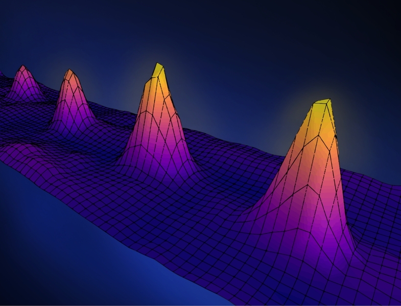
Cover Image: 3D Optical Field Distribution of a Moiré Microcavity
May 21, 2025 — Researchers Feng Liu and Chaoyuan Jin (College of Information Science and Electronic Engineering ) together with Lei Ying (College of Physics) at Zhejiang University have published a paper entitled “Moiré Cavity–Quantum Electrodynamics” in Science Advances. In this work, they introduce a moiré superlattice into cavity quantum electrodynamics and demonstrate highly efficient control of quantum‐dot single‐photon emission by means of a multilayer moiré photonic crystal. This approach offers a new route toward on‐chip quantum light sources and quantum‐internet nodes.
Research Background
Quantum emitters—such as semiconductor quantum dots—are core components of photonic quantum technologies, and their single‐photon emission efficiency directly dictates system performance in quantum information processing. Traditional optical cavities (e.g., defect cavities in photonic‐crystal slabs) exploit the Purcell effect to enhance emission, but suffer from extremely small mode volumes that require sub‐wavelength positional accuracy of the emitter relative to the field maximum. Moreover, conventional cavities’ high quality factors (Q) are highly sensitive to fabrication imperfections, forcing a trade‐off between large modal volume (spatial tolerance) and strong Purcell enhancement.
Moiré photonic crystals, formed by stacking layers with slightly mismatched lattice constants, exhibit nearly flat photonic bands and therefore, in theory, an unbounded density of optical states. By harnessing this unique dispersion, one may overcome the above limitations—achieving both high Q and large spatial mode volume simultaneously.
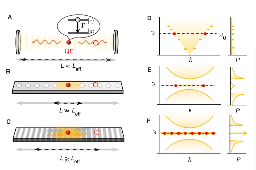
Fig. 1. Schematics of photon emission in various photonic structures. (A-C) Schematics of quantum dots in traditional Fabry-Pérot microcavities, one-dimensional photonic crystal defect cavities, and moiré photonic crystal microcavities. (D-F) The left and right panels show the dispersion relations and density of states (DOS) of quantum dots in different systems, respectively.
Key Innovations
1. Design of a High-Q Multilayer Moiré Microcavity
The team proposed a three‐layer moiré photonic‐crystal structure (Fig. 2A–C). By precisely choosing two lattice constants in each layer, they produce an extended flat band (moiré band) (Fig. 2D). Theory and measurement show that at a fixed frequency, the photonic density of states (DOS) approaches infinity, while the local density of states (LDOS) is spatially uniform—resolving the traditional conflict between high Q and large mode volume.
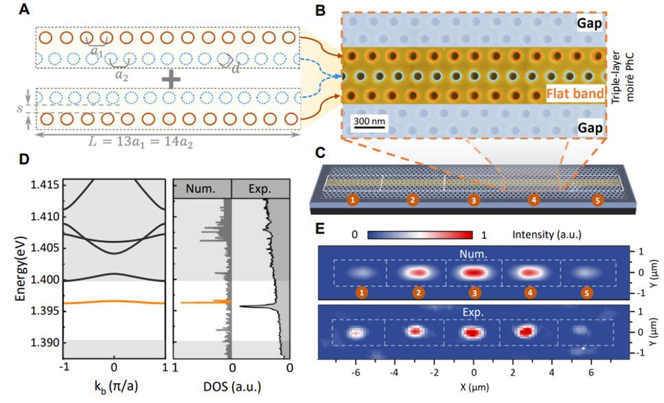
Fig. 2. (A) Unit cell of a quasi‐one‐dimensional moiré photonic crystal. (B) SEM image of a single‐cell, three‐layer moiré crystal. (C) SeM image of a moiré Phc consisting of five unit cells. (D) Comparison of experimentally measured vs. theoretically calculated DOS. (E) Comparison of simulated vs. measured spatial distribution of the optical field.
2. Cavity-Quantum Dot Coupling with Large Detuning Range of Lifetime
Integrating InGaAs quantum dots into the moiré cavity, the excitonic transition strongly resonates with a cavity mode (Fig. 3A). Hanbury Brown–Twiss (HBT) measurements reveal a single‐photon purity of 0.93 ± 0.09 (Fig. 3B). By applying a magnetic field to detune the dot–cavity resonance, the radiative lifetime can be tuned from 42 ± 1 ps up to 1,692 ± 7 ps—over a 40‐fold dynamic range (Fig. 3D).
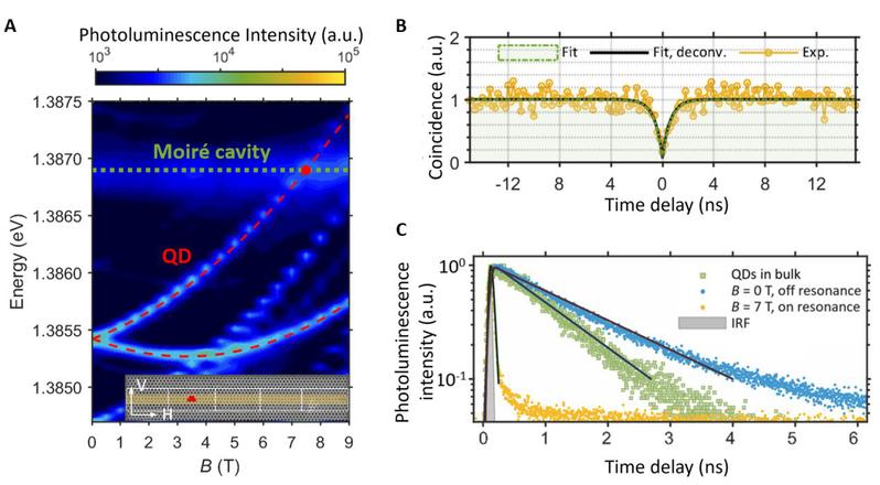
Fig. 3. (A) Magnetic‐field‐dependent photoluminescence spectra. (B) Second‐order autocorrelation (g^(2)(τ)) measurement. (C) Time‐resolved fluorescence spectra. (D) Radiative‐lifetime tuning as a function of dot–cavity detuning.
3. Silicon Compatibility and Prospects for Scalability
Using molecular‐beam epitaxy, the authors directly grew III–V quantum dots and the moiré photonic crystal on a silicon substrate, overcoming lattice‐mismatch challenges. By tuning composition and geometry, the emission wavelength can be extended into the telecom band, paving the way toward large‐scale integration on silicon‐photonic platforms.
Conclusions and Outlook
The moiré flat‐band photonic crystal uniquely combines ultrahigh density of optical states with spatial robustness, opening a new design paradigm for quantum light sources. Future work may integrate other solid‐state emitters—such as diamond color centers or 2D‐material defects—to realize dense arrays of on‐chip single‐photon sources. Furthermore, by engineering dispersion to match photonic waveguides, moiré cavities could enable efficient coupling for scalable, chip‐based quantum networks.
First authors: Yutong Wang, Qihang Ye, Junyong Yan
Corresponding authors: Chaoyuan Jin, Lei Ying, Feng Liu
Collaborating institutions: Zhejiang University; University College London; Tianjin University; Chinese Academy of Sciences, Institute of Semiconductors; Zhejiang Normal University; Anhui University
Funding: National Key R&D Program of China; National Natural Science Foundation of China; Zhejiang Provincial Natural Science Foundation; UK Engineering and Physical Sciences Research Council (EPSRC)
DOI: https://www.science.org/doi/10.1126/sciadv.adv8115