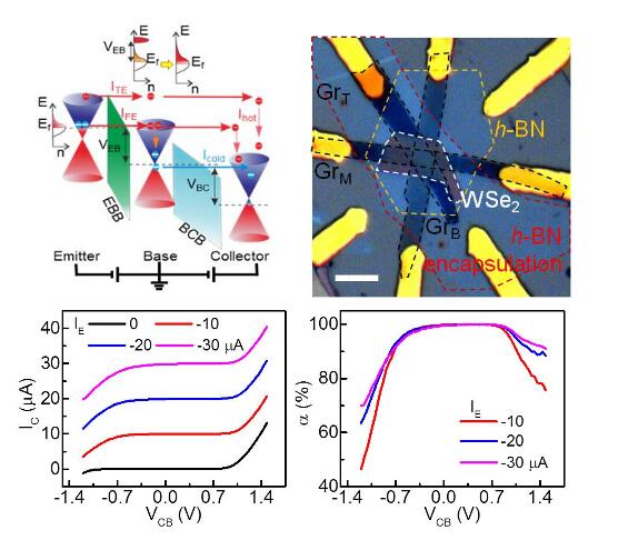
Prof. Xu Yang's group first proposed and developed a purely two-dimensional hot electron transistor (as shown in Figure 1). The device was inspired by the transfer of hot electronic amplifiers proposed in the 1960s. Its essence is to control high-energy electrons to traverse through the base of the device by ballistic transportation to ensure the high-frequency applications of the device. Historically, due to the inability to avoid perforation effects and defects of thinned traditional device materials, as well as severe scattering between interfaces, the device performance has not been able to reach desired levels for more than 50 years. However, two-dimensional material can solve the above problems due to the natural thickness of atomic layer and the clean surface. Heterojunctions of two-dimensional materials a produced by stacking, and a clean interface is obtained through continuous improvement of the process. After comparing various materials in the experiment, boron nitride with a wide bandgap and tungsten selenide with a relatively narrow bandgap are selected as two barrier layers of devices, graphene with thickness of less than 1 nm is selected as the base, which results in a transistor performance with a hot electron collection efficiency of approximately 100%. Using thin graphene as the base allows the electron transport channel to be below 1 nm, ensuring that the electron transport process is hardly scattered, and it is possible to obtain extremely high operating frequencies. A collection efficiency of more than 99.5% was observed in the experiment, as well as a clear saturation collection phenomenon.
Using HET as the object, the transport process of hot electrons in the base region can be systematically studied by changing the emitter, base, and collector materials, including inter-electron scattering (Auger and anti-Auger processes), electrons and phonons’ relaxation process. This purely two-dimensional hot electron transistor will provide entirely new experimental means for the study of high-speed two-dimensional electron gas transport and hot electron energy spectra.
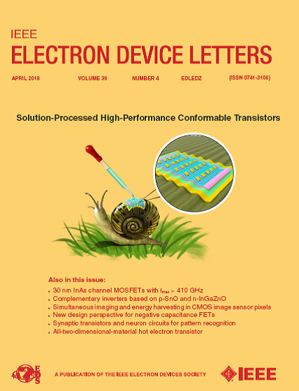
This work was recently published on the IEEE Electron Device Letters and was selected by Editor-in-Chief (Prof. Tsu-Jae King Liu at University of California Berkeley) as an Editor's Pick and highlighted on the cover of the journal (as shown in Figure 2). The link to the paper is http://ieeexplore.ieee.org/document/8304632/. In the process of this research, Yang Jianyi, Li Erping, Gao Chao, Zhang Xianmin, Yin Wenyan, Yu Xuegong, Dong Shurong, Cheng Zhiyuan, Chen Hongsheng, Xu Mingsheng, Pi Xiaodong, Zhao Yi, Zhu Haiming, Dai Daozin, Ma Xiangyang, Tong Limin, Academician Yang Deren’s team members and students have offered their help, which is highly appreciated. The research was supported by the National Natural Science Foundation of China (61674127,61474099), Zhejiang Provincial Natural Science Fund Project (LZ17F040001) and the National Key Research and Development Plan (2016YFA0200204), Zhejiang Provincial Key Laboratory of Advanced Micro-nanoelectronic Devices Intelligent Systems and Applications, ZJU - UIUC Joint Institute and the Open Fund for the State Key Laboratory of Silicon Materials.